|
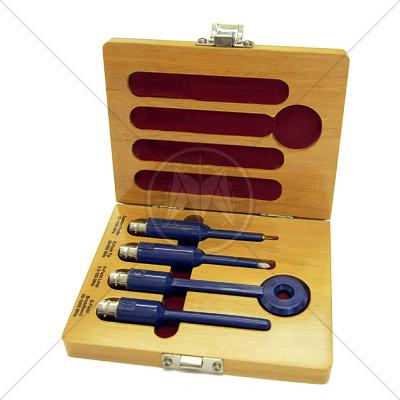
The PS-500 is a Near Field Probe set consist four probes and a custom storage case. Performance and ease of use were designed into this product. The unique design allows easy access for tight or hard to reach places while reducing the effect of hand position or cable placement.
The fine tip and the contact tip probe are a precision E-field probes that features the ability to singularly identify a problem trace or pin. The fine tip probe is designed to be extremely sensitive to distance from the source which allows easy discrimination between traces on a PCB. The unique patented design allows measurement on individual traces as narrow as 3 mils.
The contact tip probe allows direct electrical contact with the circuit. It has wider frequency range than the fine tip probe. Just like the fine tip probe the contact tip probe allow finding noise source to a trace or pin. The broadband probe is designed to identify E-fields over a broad frequency range.
The H-field probe's magnetic loop design makes it ideal for isolating sources of magnetic noise. The shielded loop construction allows measurement to minimize the effect of electrical fields.
- Complete Solution - Includes E and H field probes
- Contact tip probe - Make contact with the circuit
- Locate Noise Source - Down to a pin with the fine tip
- Lightweight - Easy to use and handle
- Small Size - Allows easy access to corners
- Sensitive to Tip Position - Ease of pinpointing source
- Immune to Hand Position - For repeatable results
- Optional preamplifier
Com-Power PS-500 Application
The PS-500 Near Field Probe Set is designed to assist in troubleshooting EMI problems both at the board level and at the component level. It is used to detect radiation from cables, cases, traces and ICs.
Typically the broadband probe is used to locate the general area of emission. Then the tip probe is used to isolate the source to a specific trace or pin. Further analysis can be done using the contact tip probe by making direct contact with the circuit and then following the noisy trace to find the cause of emissions such as a broken transmission line or impedance mismatch.
A typical use for the H-field probe is to verify the integrity of the chassis of your computer. This is done by moving the probe along the seams of the chassis which may be acting as slot antennas. This probe is also very useful for detecting magnetic noise sources such as large current switching circuits or transformers.
By utilizing the appropriate probes, potential certification problems can be discovered and addressed before expensive compliance testing is done. This saves both money and valuable time. The net result is a reduction in testing costs and a decreased time to market.
|
Probe
|
Loop
|
Broadband
|
Fine Tip
|
Contact Tip
|
|
Frequency (MHz)
|
0.3-100
|
20 -1000
|
30-600
|
300-1500
|
|
Type
|
H-field
|
E-field
|
E-field
|
E-field
|
|
Connector
|
BNC (f)
|
BNC (f)
|
BNC (f)
|
BNC (f)
|
|
Dielectric breakdown
|
1 kV
|
1 kV
|
1 kV
|
1 kV
|
|
DC input at the tip
|
N/A
|
N/A
|
N/A
|
50 VDC
|
|
Weight
|
4 oz / 113 g
|
4 oz / 113 g
|
4 oz / 113 g
|
4 / 113 g
|
Standards
|
CISPR 11 |
|
CISPR 14 - 1 |
|
CISPR 14 - 2 |
|
CISPR 14 - 2 |
|
CISPR 16 - 1 |
|
CISPR 16 - 2 |
|
CISPR 16 - 3 |
|
CISPR 16 - 4 |
|
CISPR 22 |
|
CISPR 24 |
|
IEC/TR EN 61000 - 1 - 1 |
|
IEC/TR EN 61000 - 2 - 1 |
|
IEC/TR EN 61000 - 2 - 3 |
|
IEC EN 61000 - 3 - 2 |
|
IEC EN 61000 - 3 - 4 |
|
IEC/TC EN 61000 - 3 - 5 |
|
IEC EN 61000 - 4 - 2 |
|
IEC EN 61000 - 4 - 3 |
|
IEC EN 61000 - 4 - 4 |
|
IEC EN 61000 - 4 - 5 |
|
IEC EN 61000 - 4 - 6 |
|
IEC EN 61000 - 4 - 7 |
|
IEC EN 61000 - 4 - 8 |
|
IEC EN 61000 - 4 - 9 |
|
IEC EN 61000 - 4 - 11 |
|
EN 50 081 part 1 |
|
EN 50 081 part 2 |
|
EN 55 011 |
|
EN 55 013 |
|
EN 55 014 |
|
EN 55 015 |
|
EN 55 020 |
|
EN 55 022 |
|
EN 55 024 |
|
EN 50 082 part 1 |
|
EN 50 082 part 2 |
|
EN 50 093 |
|
FCC Part 15 |
|
MIL-STD - 461E |
|