Products
- Amplifier
- Analyzer
- Antenna
- Automotive EMC
- Cable Fault Locator
- Calibrator
- Chamber / Oven
- Coupling / Decoupling (CDN)
- Curve Tracer
- Data Acquisition
- Electronic Load
- EMC / EMI
- Environmental
- ESD Simulator
- Generator
- GTEM / TEM Cell
- Harmonics & Flicker
- Hipot
- LISN
- Mains Dips & Drops
- Meter
- Oscilloscope
- PIM Test Solution
- Power Supply
- RF Field Monitor System
- Thermostream
Featured Products

California Instruments MX135-3 High Output AC Power Source 135kVA

IFI T4026-50 High Power TWT Amplifier 26.5 GHz – 40 GHz 50W
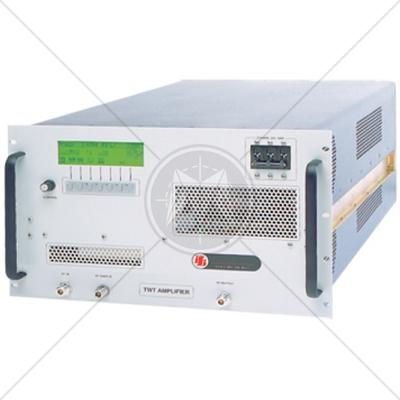
IFI T2618-50 High Power TWT Amplifier 18 GHz – 26.5 GHz 50W
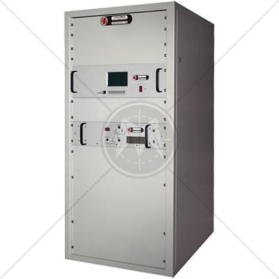
IFI TCCX2500 Tetrode Tube RF Amplifier 10 kHz – 220 MHz 2500W
California Instruments MX45-3 High Output AC Power Source 45kVA
IFI M406 Tetrode Tube RF Amplifier 10 kHz – 220 MHz 1000W